Output voltage level of TTL gate
I answered this SE EE question on June 3, 2023. This is my latest (to date) CircuitLab story dedicated to the famous TTL logic gate family.
How do we demystify TTL output stage?
TTL circuits are some of the strangest creations of circuit designers (perhaps rivaled only by ECL circuits). If we type in the Google window "transistor-transistor logic", more than 18 million pages will pop up telling us "this is so..." but we will hardly find any pages that say "why this is exactly so..." We have no choice but to try to answer our own questions.
There are two oddities in these creations - first in their input part and then in their output part. Here, the object of our attention is their output part.
Reinventing TTL output stage
I am not a circuit designer, just a "circuit thinker"... and I can only guess what the designers had in mind in the 60's. What I can do is try to reproduce their train of thought in the form of an imaginary pseudo-invention.
The idea of the complementary output stage
... is extremely simple and intuitive - to change simultaneously and in opposite directions the resistances of a voltage divider. This configuration can be thought of as two cross-fading "pull-up" and "pull-down" resistances.
Potentiometer
This idea was implemented in its simplest electromechanical form already in the 19th century as a potentiometer. A unique property of this device is that when we move the wiper, the total resistance, current and voltage remain constant; only the ratio between partial resistances and voltage drops changes...
 |
| simulate this circuit – Schematic created using CircuitLab |
... and we use one of the voltages (usually the grounded one) as an output voltage Vout. Use DC sweep simulation.

Complementary (push-pull) stage
It was implemented a century later using tubes and transistors. The only difference with the potentiometer is that the resistances are electrically controlled and non-linear.
The most logical solution in our opinion now would be for them to then use different (NPN and PNP) transistors. They should be connected with their collectors (as today MOS transistors in a CMOS pair are connected through their drains). We can name this "complementary TTL" structure CTTL:-)
I will use CircuitLab to explore the schematics below. Since they are conceptual, I propose to drive the transistors in the most straightforward way by applying two separate input voltages (Vin1 referenced to Vcc and Vin2 to ground) directly to their base-emitter junctions. Because this is inconvenient in practice, later we will combine them into a single input voltage Vin. We only want to be careful not to exceed the permissible base-emitter voltage. Let's first manually explore three typical states of this configuration.
Vin = 0 V (Vin1 = 700 mV, Vin2 = 0 V). After carefully setting these input voltages, Q1 will be on and Q2 off. A current flows through Q1, exits and passes through the load (a voltmeter with intentionally reduced to 10 k resistance). So the stage is sourcing.
 |
| simulate this circuit – Schematic created using CircuitLab |
Vin = 2.5 V (Vin1 = 750 mV, Vin2 = 712 mV). During the transition, both transistors must pass current (the output should not remain "floating") and the output voltage must be equal to half of the supply voltage. Adjust Vin1 and Vin2 carefully to achieve this condition.
 |
| simulate this circuit |
Vin = 5 V (Vin1 = 0 V, Vin2 = 700 mV). Now the roles are reversed - Q1 is off and Q2 on. A current flows through the load (a voltmeter with intentionally reduced to 10 k resistance), enters and flows through Q2. The stage is sinking.
 |
| simulate this circuit |
Vin = var (Vin1 = 750 mV - 0 V, Vin2 = 0 V - 697 mV). Finally, let's investigate the stage by a linearly varying input voltages to see the transition. Since I have used CSV voltage sources, use time-domain simulation.
 |
| simulate this circuit |
As you can see from the graph, the characteristic resembles that of the CMOS stage. It is very steep in the middle because the transistors behave as current sources at the time of switching (dynamic load) and reach the supply rails when they are on. So our "CTTL stage" is almost perfect.

Conceptual phase splitter circuit
It is time to replace the two separate input voltage sources (one of which is connected to Vcc) with just one grounded source Vin. Let's model it first with the ubiquitous voltage divider, only a little more complicated - with two constant resistors R1 and R2 and a variable resistor RQ inserted between them.
 |
| simulate this circuit |
When we vary RQ, the common current through the three resistors in series varies (unfortunately non-linearly) and the voltage drops across R1 and R2 vary as well. So if RQ is a voltage-controlled resistor, the two transistor input voltages will be controlled by the single input voltage.

Practical phase splitter
It remains only to replace the variable resistor with a transistor Q that will act as a voltage-controlled "resistor".
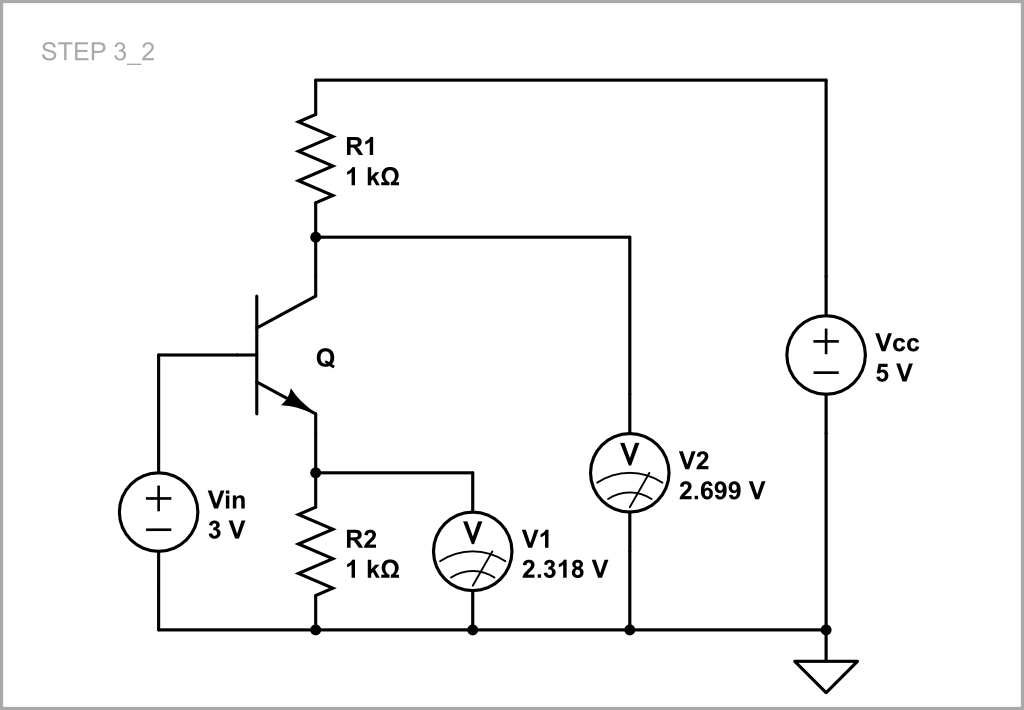 |
| simulate this circuit |
Now the voltage drops across R1 and R2 depend almost linearly on the input voltage.

Prototype of TTL output stage
However, for a number of reasons, PNP transistors were inconvenient to use, and so the designers decided to replace Q1 with another NPN transistor... and this is where the trouble starts (note that it works in active mode as an emitter follower, not as a transistor switch). Let's do it and connect the phase splitter to the NPN transistor pair...
 |
| simulate this circuit |
... and sweep Vin. But what is this significant current surge at the moment of switching?

Aha... clear! This is the moment when both transistors are "on". We need to somehow reduce the overlap and limit the current surge.
Classic TTL output stage
We notice that when Q is on, only the Q2 base-emitter junction is in parallel to Q1 base-emitter junction and that is not enough to be Q1 off. We need to insert another diode somewhere in the loop. The designers chose to put it in the emitter of Q1 apparently because the current is higher there. Then, to limit the current, let's insert a 130 ohm resistor R3.
 |
| simulate this circuit |
Now let's see how the output voltage changes.

At the moment of transition, the current is significantly reduced.

Why the HIGH output voltage is low
- A bunch of problems lead to this:
- A voltage drop is lost in the resistor R1
- Another voltage drop is lost in the resistor R3
- 0.7 V is lost in the emitter follower Q1
- Another 0.7 V is lost in the diode D
You can see it in the graph below.

How to make it high
We can "pull up" the TTL output by another resistor R4 connected to Vcc. The trick is that diode D is off and disconnects Q1 from the output.
 |
| simulate this circuit |
As you can see, the output voltage is almost 5 V but only if there is a high resistance load connected.
Comments
Post a Comment