My CircuitLab bag of tricks
I am an "inventor at heart"; so after I started working with the CircuitLab simulator, I immediately began to come up with various clever tricks, which are much easier with the simulator than in reality. Here are some of them:
- Step-by-step "building scenarios". I make them very easily, "back to front". I start with the last, most complex schematic, and gradually remove the elements from it; thus I arrive at the first, simplest schematic. I surround schematics with a gray border having the same size. Thus the same dimensions (scale) of devices are obtained and they are drawn at the same place (important for step-by-step scenarios). This representation is specific to me and serves like a "watermark". As an example, here is the first schematic in a gray frame extracted from my answer to the SE EE question Output voltage level of TTL gate.
 |
| simulate this circuit – Schematic created using CircuitLab |
- Decomposing simulations into multiple frames. My principle is "little text among many schematics" instead of the classic "little schematics among many text". In principle, a "universal" simulation with options to change many parameters should be sufficient. But beginners do not know what to do with it, or they are simply too lazy to experiment. That is why I decompose it into many separate "snapshots" with specific parameters and comment on them with a short text. The "snapshots" are hierarchically numbered in the upper left corner. This is how some kind of "CircuitLab comics" are made.
- Suppressing the graph autoscaling. I add a fake output quantity that is bigger but close to the main one. Then I delete its graph with a graphic editor.
- Simulated devices. By the help of CircuitLab we can make sophisticated experiments where to model the behavior of active devices by simple equivalent electrical devices. For example, in my answer to the Calculating resistance of a load question on SE EE, I have shown how to model the diode behavior by a dynamic resistance. Since there is no such CircuitLab element, I first emulate it with a manually controlled variable resistor.
- Manually controlled experiments performed by a "diode man", "transistor man", "op-amp man", etc. where we act as active electronic devices. For example, here is the schematic of a voltage follower implemented with an "op-amp man" (a potentiometer driven by me) that I posted in my answer to the Non-inverting op-amp question on SE EE. I name such an experiment "negative feedback game".
- Interacting "transistor men". The idea above can be developed with more than one "transistor man". I have done it in my detailed story about the famous cascode pair where two people simultaneously vary two resistances Rv and Ri.
- Generic elements. I delete the specific names of the devices in the "parameters" field because they are not needed in my conceptual schematics; they rather interfere with the understanding of the basic idea.
- "Ideal" diodes with a desired forward voltage instead real diodes, LEDs, backward-biased Zener diodes, etc. with their non-linear IV curves. See, for example, my last answer to an SE EE question about a LED indicator where LED1 and LED2 are represented by forward-biased "ideal" diodes with VF = 3 V.
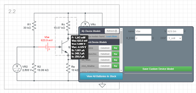
- Vbe compensated transistors. In most cases, the base-emitter voltage drop Vbe of BJT is undesired. So, we can compensate it by connecting an additional voltage source with Vbe in series. For example, I have used this biasing trick in my answer to the Why does a common base amplifier give a non inverting output? SE EE question.
- Adjusting the device values to get the results we want (solving by guessing) is a powerful technique for "man-controlled" simulation experiments. For this purpose, I open the CircuitLab parameters window and adjust the device's value by looking at the readings under the mouse or instruments (DC Live Simulation). I have used the schematic above to illustrate this "negative feedback technique"; see also the push-pull stage below.
- Conceptual transistor implemented by a voltage-to-current converter aka voltage-controlled current source (VCCS). As in the compensated transistor above, the conceptual transistor is "ideal" since there is no base-emitter forward voltage Vbe.
- Behavioral sources. This CircuitLab feature allows to flexibly set the parameters of the sources. Thus, for example, the voltage of a voltage source can copy the voltage drop across a resistor and add the "copy" to it to compensate. Or, it can follow the voltage of another voltage source (follower).
- Intentionally worsening the device resistance. CircuitLab allows us to set a lower resistance of voltmeters (initially infinity) or a higher resistance of ammeters (initially zero), to change the internal resistance of batteries, inductors, diodes, etc. Thus, measuring instruments can play the role of loads ("visualized resistors" ). The schematic is simplified and space is saved; the influence of resistance is understood. In this way, "voltage conflicts" can be removed. For example, I have used this trick in my answer to the Class AB crossover distortion diode fix SE EE question. Here I have connected two perfect ammeters to measure the collector currents Ic1 and Ic2. As a load I have used another but "worsened" ammeter IL (with a resistance increased to 100 ohm) so you do not have to worry about it burning.
 |
| simulate this circuit |
 |
| simulate this circuit |
- Intentionally decreasing the op-amp gain (up to 1) to see the role of the gain. It is very useful for understanding to explore the op-amp circuit operation with the help of CircuitLab starting with a "very real amplifier" (with very low gain) and gradually making it almost ideal (with extremely high gain). I have shown this technique in my answer to an SE EE question about the famous op-amp follower.
 |
simulate this circuit
|


Comments
Post a Comment