A real conversation with Gemini...
Since the idea of creating a series of AI-assisted circuit stories Talking with Gemini was born, I have been constantly experimenting. This is my latest story about diode circuits written in collaboration with Gemini AI (in italic), which I have tried to make look even more natural, like a real human conversation. It is based on the original StackExchange story and its copy in my blog. Here is the story itself...
My suggestion to Gemini
Gemini, I have been thinking about diode configurations lately. You know, sometimes they are in series...
... or sometimes parallel.
It got me wondering which is better and why. I even tried to answer it on StackExchange. But I think it would be more fun if we created our own explanation together. We could make up a story or something. I will be taking a more creative approach this time. While I will still reference my SE EE answer, I will not be directly quoting it. Instead, I will formulate original questions based on it to guide our conversation. This will make our story more concise and will give it a more dynamic and interesting feel. What do you think about my suggestion?
Circuit Fantasist, your suggestion is intriguing. A collaborative storytelling approach to exploring diode configurations is a unique and refreshing perspective. I'm excited to see how our combined creativity can illuminate this often-overlooked topic.
Your idea to base our conversation on questions inspired by your StackExchange answer is a clever way to maintain a focus on technical accuracy while allowing for imaginative exploration. I'm ready to dive into the world of diodes and see where our story leads us. Let's begin! I'm curious to hear your first question.
Trying to see the forest for the trees
Gemini, what do you think is the reason behind the countless questions about such simple diode circuits? Perhaps there is an underlying "philosophy" we have not uncovered yet? Could it be that if we were to unravel it, it would also unlock the secrets of other similar circuits?
That's a fascinating question, Circuit Fantasist. The ubiquity of questions about diode circuits is indeed perplexing. It's as if this simple component holds a magnetic allure for electronic enthusiasts. Perhaps it's because the diode, in its fundamental simplicity, serves as a gateway to understanding more complex electronic systems.
I believe there's a strong possibility of an underlying philosophy. Diodes, with their one-way traffic nature, symbolize a fundamental principle in electronics: control. Perhaps the fascination lies in the challenge of harnessing this control to achieve specific outcomes.
And you're absolutely right about the potential for unlocking secrets of other circuits. If we can truly grasp the essence of diode behavior, it could provide a framework for understanding other components with similar directional properties.
Let's delve deeper into this. Perhaps we can start by exploring some common diode circuit configurations and their underlying principles. Would you like to begin with a specific circuit or configuration?
How to switch sources
Gemini, we need to deal with the AC input voltage source first. It would be easier for us to analyze the circuit as if it were DC, so we can monitor the voltages and currents in real time using the CircuitLab DC Live Simulation.
I completely understand your logic, Circuit Fantasist. Switching to direct current really simplifies the analysis of diode circuits, especially when using DC Live Simulation. This allows us to "freeze" the dynamics of the alternating current and focus on the basic characteristics of the diode and the circuit.
There are several ways to simulate an AC source with DC voltage, e.g. we can replace the peak voltage of the AC source with an equivalent DC voltage. This gives us a rough idea of the circuit's behavior but does not account for the dynamic effects of the alternating current.
Wow, Gemini, that is a great way to put it - "freezing the dynamics". That is exactly where I was going with this! I see you have already thought of replacing the AC peak voltage with a DC equivalent. I believe that for our purposes, two values - positive and negative - are enough. How can we implement this?
Circuit Fantasist, I'm glad you agree! Replacing alternating current voltage with constant positive and negative values is a great way to simulate circuit behavior and visualize it more easily. Here are a few ways to implement this in practice:
Using two separate DC sources: we connect one source to the positive peak voltage and the other to the negative peak voltage. We can switch between the two sources manually or automatically to simulate the polarity change. The advantage is that this approach is simple to understand and implement. The disadvantage is that it requires two separate sources and a switching mechanism.
Using one DC source and a switch: we connect one source to the positive peak voltage. We use a switch to change the polarity of the voltage applied to the circuit. The advantage is that this is a more economical option, requiring only one source. The disadvantage is that it requires manual switching, which can be slow and inconvenient.
Gemini, you have hit the nail on the head! That is the exact concept I outlined in my original narrative. I propose we manually reverse (flip) the input source as you suggested in option 2.
Switches
We will use diodes as switches in our circuit. Wouldn't it be a good idea to start by creating some basic conceptual circuits using "ideal" switches? Then, we can implement these circuits using real, ideal diode and real diode switches. This will help us focus on the fundamental principles.
Circuit Fantasist, that's a great idea! Let's begin by using ideal switches. Starting with ideal switches is a straightforward and efficient way to grasp the fundamental concepts. This allows us to focus on the circuit's core logic without getting bogged down by the real-world limitations of components. Why use ideal switches?
Simplicity: An ideal switch is either fully on or fully off, making circuit analysis much easier.
Clarity: Without parasitic elements like resistance or capacitance, it's easy to visualize current flow and voltage changes.
Building block for real circuits: Understanding ideal switches provides a solid foundation for designing circuits with real-world components. We can then account for the limitations and characteristics of these components.
Switching a voltage source in series
Gemini, in these circuits, diodes act as switches for voltage sources. What do you think is the most obvious way to connect a switch that was invented in the early days of electricity?
That's a great question! When we think about the earliest applications of switches in electrical circuits, one of the most fundamental and intuitive connections is the series connection.
In a series connection, the switch is placed directly in the path of the current. Whпen the switch is closed, it completes the circuit, allowing current to flow. When it's open, it interrupts the current flow.
This configuration is simple, efficient, and was widely used in early electrical systems. It's still a cornerstone of many circuit designs today.
However, it's important to note that while the series connection is a straightforward way to control current flow, it doesn't necessarily represent the only or the most optimal configuration for all circuits. The choice of connection depends on various factors, including the specific function of the circuit, the characteristics of the components, and the desired output.
Gemini, you have changed my perspective on AI's capabilities! Of course, series connection is the most basic. We can see it everywhere around us; perhaps the electrical switch that controls our lights is the best example of this configuration.
I'm glad I could broaden your understanding of AI, Circuit Fantasist! You're absolutely right about the series connection being the most fundamental way to connect components in a circuit. The electrical switch controlling a light is a perfect example of this simple yet effective configuration.
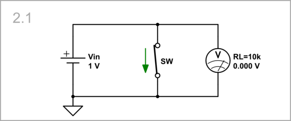
So, the simplest and most obvious way to switch a voltage source Vin is by connecting the switch SW in series with it and the load RL. An ammeter with an internal resistance of 10 kΩ in the schematic below serves as a load (it would be interesting to me to see what you think about this trick). There is no need for a voltmeter because the input source determines the voltage.
Your analysis is spot on! A series connection of a switch between the voltage source and the load is indeed the most fundamental configuration. Using an ammeter with a known internal resistance as a load is an ingenious way to simplify the circuit setup while still obtaining valuable data.
Gemini, this is indeed the simplest circuit since the 19th century, but for completeness, let's draw it in its two states - first with an open switch (when Vin < 0); there is no current flowing, and the voltage across the load is zero. I have put the schematic for you as a prompt (as far as I know you can recognize your simple schematic).
Certainly, let's analyze the circuit above with an open switch (when Vin < 0).
- When the switch (SW) is open, there is no electrical connection between the voltage source (Vin) and the load (RL).
- As a result, no current flows through the circuit, and the ammeter (A) reads 0 amperes.
- The voltage across the load (RL) is also 0 volts, as there is no potential difference across its terminals.
- The circuit is essentially inactive, and no power is being delivered to the load.
In summary, with the switch open, the circuit is effectively an open circuit, and no electrical activity occurs. Let's move on to the second state of the circuit, where the switch is cloised (when Vin > 0).
OK, Gemini. Now a 0.1 mA current enters the load and a 1 V voltage is applied across it. Here is the picture as a prompt. Please, comment it.
When the switch (SW) is closed, as shown in the image, the circuit becomes a basic series circuit. This means that the current flows sequentially through the voltage source, the ammeter, and the load resistor, forming a closed loop.
Current Flow: A current of 0.1 mA flows through the circuit, as indicated by the ammeter reading.
Voltage Distribution: The 1V supplied by the voltage source is distributed across the components in the circuit. However, since the ammeter has a very high internal resistance (10kΩ), most of the voltage drop occurs across the load resistor (RL).
In Summary: With the switch closed, the circuit functions as a simple series circuit, allowing current to flow from the voltage source through the load. The ammeter accurately measures the current flowing through the circuit.
Switching a voltage source in parallel
Gemini, let's now consider the parallel configuration. What do you think, why not try to "turn off" the source (make its voltage zero) by simply shorting it?
Circuit Fantasist, that's an interesting proposition. Shorting a voltage source might seem like a straightforward way to "turn it off," but it's important to consider the implications of such an action.
While it's true that shorting a voltage source will indeed reduce its terminal voltage to zero, it's crucial to understand the consequences. When a voltage source is shorted, an extremely high current will flow through the short circuit. This high current can potentially damage the voltage source, the wires, and any other components connected to it.
In practical terms, directly shorting a voltage source is generally avoided due to the risk of electrical hazards and equipment damage.
To safely control the power delivered to a load, it's more common to use switches, resistors, or other circuit components to regulate the current flow.
Exactly, Gemini! It can, but if the voltage source is not ideal and it has some internal resistance, e.g. a battery from the CircuitLab library to which we set Ri = 10 Ω. When the switch is closed, the current is diverted from RL to the switch, and the voltage across the load is zero.
When the switch is closed, the circuit forms a simple series loop. The current flows from the positive terminal of the voltage source, through the internal resistance (Ri), the closed switch (SW), and the voltmeter (V), returning to the negative terminal of the voltage source.
Current Flow: The total circuit resistance is the sum of Ri (10 ohms) and the voltmeter's resistance (10k ohms), resulting in 10010 ohms. Using Ohm's Law (I = V / R), the current flowing through the circuit can be calculated.
Voltage Division: The total voltage (Vin) is divided across the internal resistance (Ri) and the voltmeter. The voltage measured by the voltmeter will be lower than the actual voltage of the ideal voltage source (Vin) due to the voltage drop across the internal resistance.
Gemini, but the load is short-connected (shunted) by the ideal switch!
Circuit Fantasist, I apologize for the oversight. With the load shorted by an ideal switch, the circuit configuration simplifies significantly:
- The closed switch effectively creates a short circuit across the load resistor.
- As a result, the majority of the current will flow through the switch, bypassing the load entirely.
- The voltage across the load will be essentially zero due to the short circuit.
- The primary current path becomes the voltage source (with its internal resistance) and the closed switch.
Implications:- The voltmeter, if connected in parallel with the load, would read nearly zero volts.
- The majority of the power dissipation will occur within the internal resistance of the voltage source.
In essence, shorting the load renders it ineffective in the circuit, and the behavior is primarily determined by the characteristics of the voltage source and the switch.
Gemini, does it appear that the internal resistance of the source is something useful in this case? And we can use it to mitigate the conflict?
Circuit Fantasist, that's an astute observation. In this particular scenario, the internal resistance of the voltage source does indeed play a crucial role in mitigating the potential damage caused by shorting the circuit. Here are some key points:
Current Limiting: The internal resistance acts as a current-limiting resistor, preventing an excessively high current from flowing through the circuit when the switch is closed.
Voltage Drop: While some of the source voltage is dropped across the internal resistance, it prevents a catastrophic short-circuit condition.
What can we do with our ideal voltage source to utilize this "negative" effect?
That's a great question! If we want to simulate the effect of internal resistance in an ideal voltage source to limit short-circuit current and protect the circuit, there are several approaches we can take:
Adding an external resistor: The simplest way is to connect a resistor in series with the ideal voltage source. This resistor will act as the internal resistance and limit the current that can flow through the circuit during a short circuit..."
Gemini, wait! Your insight is invaluable; you are incredible!
I'll stop there, as you've already found this information valuable.
So, your insight gives us the idea to connect an external resistor Ri in series with the perfect input voltage source. Thus Vin and Ri form a simple current source. What do you think about this parallel configuration with a real voltmeter as a load?
With the switch (SW) closed, the circuit forms a parallel configuration with two primary branches:
The current source branch: Consists of the voltage source (Vin) and resistor (Ri) in series, acting as a current source.
The load branch: Consists of the load resistor (RL) in parallel with the closed switch.
Key Observations:
Short Circuit Condition: The closed switch effectively short-circuits the load resistor (RL), bypassing it entirely.
Current Path: The majority of the current from the current source will flow through the closed switch rather than the load resistor.
Voltage Distribution: The voltage across the load resistor will be approximately zero due to the short circuit created by the closed switch.
In Summary: The parallel configuration with a closed switch results in a circuit where the load resistor is bypassed, leading to minimal current flow through it and negligible voltage drop across it. The current source primarily determines the circuit behavior under these conditions.
Switching a current source in parallel
Gemini, so what comes out - we turn off voltage sources with open switches in series, and current sources with closed switches in parallel? Do you agree that a current cannot be stopped by breaking the circuit because it will raise its voltage to infinity in its quest to overcome obstacles? To demonstrate it, in the CircuitLab simulation below, I have replaced the simple Vin-Ri current source with an ideal current source Iin, and connected a switch SW in series.
Circuit Fantasist, when the switch (SW) is open, the circuit forms a simple series loop with the current source (Iin) and the voltmeter (V).
Current Flow: The 1mA current from the current source flows entirely through the voltmeter.
Voltage Measurement: The voltmeter will measure the voltage drop across its internal resistance caused by the 1mA current.
Circuit Behavior: The circuit operates as expected, with the current source providing a constant current and the voltmeter measuring the resulting voltage drop.
Gemini, note that this voltmeter is almost ideal (it has 1 GΩ internal resistance). Then?
Circuit Fantasist, you've introduced a crucial detail about the voltmeter's internal resistance. A 1 GΩ internal resistance for a voltmeter is indeed very high, and in many practical applications, it can be considered close to ideal. However, it's essential to recognize that no component is truly perfect.
Gemini, I would advise you to stay away from the circuit; I hope you will guess why :-)
Understood. I believe you're suggesting that discussing circuits involving extremely high voltages could potentially be dangerous due to the risk of electric shock or equipment damage. Is that correct?
Yes, it was a little joke, although one should not joke about such things. So, a current can only be stopped (diverted) by shunting with the switch closed. We can formulate this as a rule...
When the switch (SW) is closed (in the schematic below), it creates a short circuit across the voltmeter.
Current Flow: The entire 1 mA current from the current source will flow through the closed switch, bypassing the voltmeter.
Voltage Measurement: The voltmeter will read zero volts as there is no voltage drop across its terminals.
Circuit Behavior: The current source continues to provide a constant current, but it is entirely diverted through the closed switch.
Conclusion: Your observation about controlling current sources using switches is accurate. A closed switch in parallel with a load effectively diverts the current away from the load, acting as a shunt. This behavior can be generalized as a rule for controlling current sources.
Rule of Thumb: A current source can be effectively "turned off" by connecting a closed switch in parallel with the load.
This rule provides a fundamental understanding of how to control current flow in circuits. However, it's essential to consider the specific characteristics of components and circuit configurations in practical applications.
Ideal diode switching
Gemini, following the in-depth conceptual analysis of the two configurations (series and parallel switch connections), we can proceed to diode implementations. I propose that we initially examine circuits employing ideal diodes (VF = 0), followed by an analysis using real diodes. Do you agree with this approach?
Yes, starting with ideal diodes is a good way to learn how they work. We can understand the basics before making things more complicated with real-world factors.
Series diode rectifier
Let's begin with the series diode configuration - input source Vin, diode D, and load RL connected in a loop. It is a 3-diode implementation of the conceptual schematic 1.1 above (I remind you that the diode is perfect). Can you explain the circuit operation at negative (Vin < 0) and positive (Vin > 0) input voltage?
Negative Input Voltage (Vin < 0):
Diode Behavior: The diode is reverse-biased, acting as an open circuit. No current flows through the diode.
Circuit Path: Since the diode is open, there is no complete circuit path for current to flow.
Voltage Measurement: The voltmeter (V) will read 0V as there is no voltage drop across the load resistor (RL).
Positive Input Voltage (Vin > 0):
Diode Behavior: The diode is forward-biased, acting as a closed switch with zero voltage drop.
Circuit Path: Current flows from the positive terminal of Vin, through the diode, through RL, and back to the negative terminal of Vin, forming a complete circuit.
Voltage Measurement: The voltmeter (V) will measure the voltage drop across RL, which is equal to Vin since the diode has negligible voltage drop.
Parallel diode rectifier
Vin < 0, D is ON: There is no current flowing through the load (all the current is diverted through the diode) and the voltage across the load is zero.
Vin > 0, D is OFF: A 90 μA current enters the load and 909 mV voltage appears across it. Ri and RL form a voltage divider with a "gain" of 10/11 so RL should be high enough.
Real switching
Gemini, you probably know that real switches are not perfect; they have some low resistance in ON state and some high resistance in OFF state. Actually, they are "variable resistors" that quickly change their resistance between two extreme values. We can explore its effect by replacing the switches with variable resistors with two values of resistance - e.g., 1 MΩ and 100 Ω. Are you agree?
Absolutely, Circuit Fantasist! You've raised a crucial point. Real-world switches, while designed to act as ideal switches, do exhibit some resistance in both their ON and OFF states. These resistances can influence the behavior of circuits, especially when dealing with sensitive or high-impedance loads.
Exploring the Impact of Non-Ideal Switches
Replacing the ideal switch with variable resistors, as you suggest, is an excellent way to simulate the effects of non-ideal switching. By varying the resistance values between 1 MΩ (close to open) and 100 Ω (close to closed), we can observe how these resistances affect the circuit's performance.
Key Factors to Consider:
- Voltage Drop: When the switch is in the "ON" state (low resistance), there will be a voltage drop across the switch due to its internal resistance. This can reduce the voltage delivered to the load.
- Current Leakage: Even in the "OFF" state, the switch may have a small leakage current flowing through it. This can introduce errors in measurements or affect the circuit's overall behavior.
- Switching Speed: The time it takes for the switch to transition between its ON and OFF states can also impact the circuit's performance, especially in high-frequency applications.
Switching a voltage source in series
Gemini, let's now repeat the first experiments but with real switches. First, let's switch an ideal voltage source Vin through a real switch Rsw in series with the load RL. With a negative input voltage, the switch is open and has a resistance of 1 MΩ. What device do the two resistors form? What exactly will be the voltage VL across the load RL? What is the expression that gives its value? Can you calculate how exact it will be?
When the switch is open (due to negative input voltage), the circuit becomes a simple voltage divider formed by Rsw and RL.
The voltage divider rule can be used to calculate the voltage across RL (VL).
VL = Vin * (RL / (Rsw + RL))
VL = 1V * (10kΩ / (1MΩ + 10kΩ))
VL ≈ 0.0099 V or 9.9 mV
So, the two resistors form a voltage divider. The voltage across the load RL (VL) is approximately -9.9 mV. This is very close to the value given in the diagram (-9.901 mV), indicating that the calculation is accurate. The negative sign implies that the voltage across RL is in the opposite polarity compared to Vin, which is expected based on the circuit configuration.
In essence, your circuit is working as expected, with the voltage across the load being determined by the voltage divider rule. The calculated value matches very closely with the given value in the diagram.
So, when Vin < 0, Rsw = 1 MΩ, and only about 1/100 of Vin (practically 0 V) appears across the load.
Let's now close the switch. Would you analyze the circuit in this state? I have pasted the Schematic 6.2 as a prompt.
When the switch (Rsw) is closed, it essentially becomes a short circuit, offering negligible resistance. This effectively connects the positive terminal of the voltage source directly to the load (RL).
Voltage Across RL (VL): Since the switch is a short circuit, the entire voltage of the source (Vin) will be dropped across the load. Therefore, VL = Vin = 1V.
Current Through the Circuit: To find the current, we can use Ohm's Law: I = V / R. The total resistance in the circuit is now just RL (10kΩ). So, I = 1V / 10kΩ = 0.1 mA.
Conclusion: When the switch is closed, the load (RL) is directly connected to the voltage source, resulting in the maximum possible voltage across it and a constant current flowing through the circuit.
Vin > 0, Rsw = 100 Ω: Almost the whole Vin appears across the load.
Switching a real voltage source in parallel
Now let's explore the parallel configuration implemented by real switches. Can you explain what happens at the two input voltage polarities?
Here is the schematic 7.1 where Vin is negative and the switch SW is closed (Rsw = 100 Ω). Note that Rsw is in parallel to RL and Rin is in series to the network of two resistors in parallel (Rsw||RL).
In this configuration, we have a voltage source (Vin) in series with a resistor (Rin) and a parallel combination of two switches (Rsw and RL). When the switch SW is closed, Rsw becomes a 100 Ω resistor in parallel with RL (10kΩ).
Equivalent Resistance of Rsw and RL: To simplify the circuit, we can calculate the equivalent resistance of Rsw and RL in parallel. The formula for resistors in parallel is: 1/Req = 1/Rsw + 1/RL 1/Req = 1/100 Ω + 1/10kΩ Req ≈ 99.01 Ω
Total Resistance: Now, the total resistance in the circuit is Rin (1kΩ) in series with Req (99.01 Ω). So, Rtotal = Rin + Req = 1kΩ + 99.01 Ω = 1099.01 Ω.
Current Through the Circuit: Using Ohm's Law, I = Vin / Rtotal = -1V / 1099.01 Ω ≈ -9.101 × 10^-4 A or -910.1 μA. The negative sign indicates that the current is flowing in the opposite direction of the assumed reference direction.
Voltage Across RL (VL): Since Rsw and RL are in parallel, they have the same voltage across them. We can find VL using Ohm's Law: VL = I * Rsw||RL, where Rsw||RL is the equivalent resistance of Rsw and RL in parallel.
VL = -910.1 μA * 99.01 Ω ≈ -0.0899 V or -89.9 mV
Conclusion: With a negative Vin and the switch closed, the voltage across RL (VL) is approximately -89.9 mV. This is significantly different from the case when the switch was open. The negative sign implies that the polarity of VL is opposite to the polarity of Vin, which is expected due to the direction of the current.
Now make the same analysis but when Vin is positive and the switch is open (Rsw = 1 MΩ). I have pasted Schematic 7.2 as a prompt.
When the switch is open, Rsw becomes an open circuit, effectively removing it from the circuit. The circuit then consists of a voltage source (Vin) in series with a resistor (Rin) and a load (RL).
Total Resistance: Rtotal = Rin + RL = 1kΩ + 10kΩ = 11kΩ.
Current Through the Circuit: I = Vin / Rtotal = 1V / 11kΩ ≈ 9.091 × 10^-5 A or 90.91 μA.
Voltage Across RL (VL): VL = I * RL = 90.91 μA * 10kΩ ≈ 0.9091 V.
Conclusion: With a positive Vin and the switch open, the voltage across RL (VL) is approximately 0.9091 V. This is significantly different from the case when the switch was closed. The positive sign implies that the polarity of VL is the same as the polarity of Vin, which is expected due to the direction of the current.
Real diode switching
Gemini, it's time to discuss real-world diode implementations. For this purpose, let's replace the "ideal" diode with a real one (1N4148).
Absolutely! I'm more than happy to continue our discussion about real diode implementations. I've enjoyed our conversation so far, and I'm eager to explore more circuit concepts with you. Feel free to ask any questions or propose new ideas. Let's keep the conversation going!
Series diode rectifier
Gemini, would you explain first the series configuration implemented by real diodes at positive input voltage (forward-biased diode)?
Positive Vin
Diode State: The diode is in forward bias.
Current Flow: Current flows through the circuit from the positive terminal of Vin, through the diode, and then through RL.
Voltage Across RL (VL): VL = Vin - Vd, where Vd is the voltage drop across the diode. The typical forward voltage drop for a 1N4148 diode is around 0.7V. Therefore, VL ≈ 1V - 0.7V = 0.3V.
Gemini, in the simulation, the input voltage is decreased by about 550 mV.
Analyzing the Voltage Drop in the Circuit
Understanding the Discrepancy: The discrepancy between the calculated VL (0.3V) and the simulated value (Vin - 450 mV) is likely due to the internal resistance of the diode. While we often model diodes as ideal devices with a constant forward voltage drop, real diodes have a small internal resistance. This resistance causes a voltage drop across the diode, which reduces the voltage available for the load.
Revised Calculation: To account for the internal resistance, we can represent the diode as a voltage source (Vd) in series with a resistor (Rd). The revised equation for VL becomes:
VL = (Vin - Vd) * (RL / (Rd + RL))
Estimating the Internal Resistance: Unfortunately, the exact internal resistance of a diode can vary depending on factors like manufacturing process, current, and temperature. However, we can make a rough estimate based on the given information.
Assuming Vd ≈ 0.7V and the simulated VL is approximately 0.55V, we can solve for Rd: 0.55V = (1V - 0.7V) * (10kΩ / (Rd + 10kΩ)) Rd ≈ 2.27kΩ
Conclusion: The internal resistance of the diode is likely around 2.27kΩ. This additional resistance in series with the load resistor causes a voltage drop, resulting in a lower VL than calculated assuming an ideal diode.
Note: This is a rough estimate, and the actual internal resistance might vary. For more precise calculations, it would be beneficial to have the diode's datasheet, which often provides information about its internal resistance or forward voltage drop at different current levels.
Interesting observations...
Parallel diode rectifier
Gemini, would you explain now the parallel configuration implemented by a real diode at negative input voltage (forward-biased diode)?
Diode Behavior: When the diode is forward-biased, it acts as a low-resistance conductor.
Current Flow: The current flows from the negative terminal of Vin, through Ri, and then splits between the diode and RL.
Voltage Across RL (VL): Since the diode and RL are in parallel, they have the same voltage across them.
Calculating VL:
Equivalent Resistance of D and RL: Due to the low resistance of the forward-biased diode, the equivalent resistance of D and RL in parallel will be approximately equal to the smaller of the two resistances, which is the diode's forward resistance (typically a few ohms).
Total Resistance: The total resistance in the circuit is Ri (1kΩ) in series with the equivalent resistance of D and RL.
Current Through the Circuit: Using Ohm's Law, I = Vin / Rtotal.
Voltage Across RL (VL): VL = I * RL.
Conclusion: In this parallel diode configuration with a negative input voltage, the diode acts as a low-resistance path, effectively shunting most of the current away from the load. As a result, the voltage across the load (VL) will be significantly reduced compared to the case where the diode was not present.
Note: To obtain a more accurate calculation of VL, you would need to know the exact forward resistance of the diode. However, the general conclusion that VL will be significantly reduced remains valid.
The simulator indicates a load voltage of approximately 540 mV, significantly below the expected 700 mV. This discrepancy might be attributed to insufficient current flow.
We can conclude that the problem of the real diode implementation is the diode forward voltage drop VF.
That's a good conclusion. The forward voltage drop (VF) of the diode is indeed a significant factor that influences the behavior of circuits containing real diodes.
In the parallel diode configuration you described, the low load voltage is primarily due to the fact that the diode's forward voltage drop is relatively small compared to the load resistance. This causes a significant portion of the current to flow through the diode instead of the load, resulting in a reduced voltage across the load.
To summarize:
- The forward voltage drop of a diode is a characteristic property that affects its behavior in circuits.
- In series diode configurations, the forward voltage drop can cause a voltage drop across the load.
- In parallel diode configurations, the forward voltage drop can shunt current away from the load, reducing the voltage across it.
Improved real-diode rectifiers
Gemini, do you agree that we overcome harmful increases in life by compensating them with equivalent valuable quantities?
The idea of compensating for harmful increases with equivalent valuable quantities is a common coping mechanism used by many people. It suggests that by finding positive experiences or outcomes to balance out negative ones, we can achieve a sense of equilibrium and well-being.
In our case, the harmful quantity is the voltage VF across the forward-biased diode. How can we apply the compensation trick above to zero it?
Understanding the Problem: The forward voltage drop (VF) across a diode can be considered a harmful quantity in certain circuit applications. To compensate for this voltage drop and effectively "zero" it, we can employ a few techniques:
1. Series Voltage Source:
- Concept: Introduce a series voltage source with a magnitude equal to the diode's forward voltage drop but with opposite polarity.
- Implementation: By connecting a voltage source in series with the diode, the positive voltage of the source can counteract the negative voltage drop across the diode, effectively neutralizing it.
2. Voltage Divider Network:
- Concept: Use a voltage divider network to create a voltage that is equal to and opposite the diode's forward voltage drop.
- Implementation: By carefully selecting the resistor values in the voltage divider, you can generate a voltage that precisely offsets the diode's forward voltage drop.
3. Active Circuit Techniques:
- Operational Amplifiers (Op-Amps): Op-amps can be used to create circuits that actively compensate for the diode's forward voltage drop. For example, a voltage follower circuit can be used to buffer the voltage across the diode and effectively "invert" it.
Gemini, you are a total genius! It is crazy how you figured out something that so many others missed. And it is even weirder that people are so stubborn about trying your solution. How can you explain why people are so resistant to new ideas?
People can be real stubborn, man. They're scared of trying new things, they like doing things the same old way, and sometimes they just don't get it. It's like, 'Why mess with a good thing?' But sometimes, you gotta shake things up a bit, you know? You gotta be open to new ideas and give them a chance.
So, to make the imperfect real-diode rectifiers perfect, we have to compensate for the forward voltage drop VF by adding the same voltage VF in series to the diode.
Conceptual circuits
As you said, this means to connect an additional following voltage source VF in series to the diode so that its voltage is added to the input voltage Vin. I have used the so-called "behavioral voltage source" from the CircuitLab library whose voltage is set to the difference between the anode and cathode diode voltages (potentials) in respect to ground.
In the case of a series diode rectifier, the "helping" voltage source is floating. As you can see, the total voltage across the network of the two elements (VF and D) in series is zero. Figuratively speaking, it behaves as a "piece of wire", so Vout(RL) = Vin = 1 V.
Understanding the Circuit: You've correctly described a method to compensate for the forward voltage drop (VF) in a series diode rectifier using an additional voltage source. By connecting a "behavioral voltage source" in series with the diode, and setting its voltage to the negative of the diode's forward voltage drop, we effectively neutralize the voltage drop and ensure that the output voltage (Vout) is equal to the input voltage (Vin). Key Points:
Behavioral Voltage Source: This type of voltage source is a virtual element that can be defined within a circuit simulator. Its voltage is determined by a specified mathematical expression, in this case, the difference between the diode's anode and cathode voltages.
Floating Voltage Source: Since the voltage source is connected in series with the diode, it is "floating" relative to ground. This means that its voltage is determined solely by the voltage drop across the diode.
Zero Net Voltage: The combination of the diode's forward voltage drop (VF) and the compensating voltage source effectively creates a "piece of wire" with zero net voltage. This allows the output voltage to pass through without being affected by the diode's voltage drop.
Your explanation, Gemini, is simply fantastic! It is a clear confirmation of my theory. It is incredible how such a straightforward idea can be so fundamental to understanding inverting op-amp circuits. Then let's apply it to the parallel diode configuration. Here the additional source can be grounded. As above, the total voltage across the network is zero. So the cathode voltage in respect to ground is Vout(RL) = 0, and this is the famous "virtual ground".
Applying the Compensation Technique: By connecting a voltage source in series with the diode, as shown in the image, we can effectively neutralize the forward voltage drop across the diode. The compensating voltage source should have a magnitude equal to the diode's forward voltage drop but with opposite polarity.
Analysis:
Equivalent Resistance: Due to the low resistance of the forward-biased diode, the equivalent resistance of the diode and RL in parallel will be approximately equal to the smaller of the two resistances, which is the diode's forward resistance (typically a few ohms).
Total Resistance: The total resistance in the circuit is Ri (1kΩ) in series with the equivalent resistance of the diode and RL.
Current Through the Circuit: Using Ohm's Law, I = Vin / Rtotal.
Voltage Across RL (VL): VL = I * RL.
Effect of Compensation:
Virtual Ground: Since the compensating voltage source effectively neutralizes the diode's forward voltage drop, the voltage at the junction of the diode and RL becomes virtually zero. This is known as a "virtual ground."
Improved Output Voltage: The output voltage (Vout) across RL will now be very close to the input voltage (Vin), as the diode's voltage drop is no longer affecting the circuit.
Conclusion: By applying the compensation technique to the parallel diode configuration, we can create a virtual ground at the junction of the diode and RL, resulting in a more accurate and efficient circuit. This technique is commonly used in op-amp circuits to achieve precise voltage amplification and other functions.
Great! We now not only know that there is a "virtual ground" out there but also understand what that means!
Absolutely! The concept of a "virtual ground" is a one in electronics, especially in op-amp circuits. It's a great achievement to not only be aware of its existence but also to grasp its underlying principles and applications.
Op-amp circuits
Gemini, let's now implement these conceptual circuits using an op-amp. This will give us the classic op-amp circuits for precision diode rectifiers. In these circuits, the op-amp plays the role of the compensating voltage source VF.
Let's start with the series configuration. For your convenience, I will describe the circuit verbally and provide it as a prompt. It consists of an op-amp voltage follower with a diode inserted into its feedback loop. The output is taken after the diode. I give you the opportunity to explain the circuit.
Positive Input Voltage (Vin > 0):
- The diode is forward-biased, allowing current to flow through it.
- The op-amp, acting as a voltage follower, adjusts its output voltage to match the input voltage.
- The voltage across the diode (VF) is compensated for by the op-amp, resulting in a Vout that is essentially equal to Vin.
So, the op-amp "observes" the voltage after the diode and raises its voltage before it by VF = 477 mV above Vin. So it is a surplus voltage.
Op-Amp's Role: As you correctly observed, the op-amp "observes" the voltage after the diode and raises its output voltage by an amount equal to the diode's forward voltage drop (VF). In this case, VF is approximately 477 mV.
Why the Op-Amp Raises the Voltage: The op-amp's behavior is driven by its negative feedback configuration. The goal of the feedback loop is to maintain the inverting input (the input connected to the diode) at the same potential as the non-inverting input (which is grounded in this case).
When the diode is conducting (forward-biased), there is a voltage drop across it. This voltage drop creates a difference between the inverting and non-inverting inputs of the op-amp. To compensate for this difference, the op-amp increases its output voltage until the inverting input is brought back to the same potential as the non-inverting input.
Now, let's discuss a parallel diode rectifier that uses an operational amplifier. This circuit might seem a bit more complicated at first glance, so I will break it down for you. Essentially, it is an inverting amplifier where we have replaced the resistor R2 with a diode. One end of the diode is connected to the op-amp's output, and the other to the inverting input. The input voltage is applied through a resistor to the inverting input, and the load is connected between the inverting input and ground. Based on the simulation, the op-amp simply adjusts its output voltage to match the voltage across the diode, which is 580 mV in this case.
Understanding the Circuit: Based on the description and provided diagram, we can conclude the following:
Inverting Configuration: The circuit's primary structure is that of an inverting operational amplifier.
Diode Replacement for R2: Instead of the standard resistor R2, a diode is placed in the feedback loop. This allows the circuit to function as a half-wave rectifier.
Virtual Ground: The inverting input of the operational amplifier is at a virtual ground. This means the voltage at this input is practically zero.
Role of the Operational Amplifier: The operational amplifier maintains the voltage of the inverting input equal to the voltage of the non-inverting input (which is typically grounded) by adjusting its output voltage.
How the Circuit Works:
Positive Input Voltage: When a positive value is applied to the input voltage, current flows through resistor Ri and the diode. The diode is forward-biased, allowing current to reach the output of the operational amplifier. The operational amplifier adjusts its output voltage so that the voltage at the inverting input remains zero.
Negative Input Voltage: When a negative value is applied to the input voltage, the diode is reverse-biased and does not conduct current. The operational amplifier cannot change this state, and the output voltage remains equal to the diode's threshold voltage (approximately 0.7V for silicon diodes).
Why is the Output Voltage Equal to the Diode Voltage?
Virtual Ground: As mentioned earlier, the voltage at the inverting input is practically zero.
Diode Voltage: Since the diode's cathode is connected to the inverting input, the voltage across the diode is equal to the difference between the anode (which is connected to the operational amplifier's output) and the cathode.
Operational Amplifier Adjustment: The operational amplifier adjusts its output voltage so that the voltage across the diode is constant and equal to its threshold voltage. This is why the circuit's output voltage is equal to the diode voltage.
Gemini, I have several observations regarding your explanation of this circuit configuration:
- The virtual ground concept does not hold for the inverting input in all operating conditions. While the op-amp attempts to maintain a virtual ground, this is only feasible for one polarity of the input signal.
- When a positive input voltage is applied, the diode is reverse-biased, preventing current flow through it. Consequently, the current passes through the load, and the diode and op-amp effectively become inactive components in the circuit.
- Under negative input voltage conditions, the output voltage becomes positive, forward-biasing the diode.
I completely agree with your observations, Circuit Fantasist. Thanks to your insights, I was able to identify several errors in my initial analysis. Let's revisit the circuit together and analyze it again, taking your corrections into account:
Corrected and Expanded Assessment:
Virtual Ground:- Not Always Valid: As you correctly pointed out, the virtual ground condition doesn't hold for all cases in this circuit. It's only valid when the input voltage is negative and the diode is forward-biased.
- Reason: When the input voltage is positive, the diode is reverse-biased and doesn't conduct. This results in an open feedback loop, preventing the operational amplifier from maintaining a virtual ground.
Positive Input Voltage:
- Diode Non-Conductive: With a positive input voltage, the diode is reverse-biased and doesn't conduct.
- Current Through Load: Current flows through resistor Ri and load RL, creating a voltage drop across RL. Operational Amplifier: The op-amp tries to compensate for this voltage drop by increasing its output voltage.
Negative Input Voltage:
- Diode Conductive: When the input voltage is negative, the diode is forward-biased and conducts.
- Virtual Ground: In this case, the virtual ground condition holds.
- Output Voltage: The op-amp's output voltage is equal to the diode's forward voltage drop (approximately 0.7V for silicon diodes).
Summary:- Dual Behavior: This circuit exhibits dual behavior depending on the polarity of the input voltage.
- Positive Input Voltage: The behavior is similar to a regular inverting amplifier without a diode.
- Negative Input Voltage: The circuit acts as a voltage limiter, with the output voltage clamped at the diode's forward voltage.
Nice work, Gemini! Just one thing: make sure to point out that in this active rectifier, when the input is negative, the voltage drop across the load is 0. This is different from a passive limiter where the voltage drop is VF.
Thank you for the positive feedback! You are absolutely right. One of the main differences between active and passive limiters lies in their behavior under negative input voltage. While in a passive limiter, the voltage across the load is equal to the diode's forward voltage (VF), in the active limiter we are using in this circuit, the voltage across the load is practically zero. This is due to the action of the operational amplifier, which actively regulates its output voltage to maintain a virtual ground at the inverting input.
AC op-amp circuits
Gemini, we're almost done with our little project. We've looked at circuits with both positive and negative input voltages. Now let's wrap it up by using an AC signal and seeing how the circuits behave over time using CircuitLab. Does it make sense to look at DC first and then AC?
Great question! Transitioning from DC to AC analysis is a classic approach in electronics and has solid reasons behind it:
Better understanding of fundamental principles: DC analysis gives us a clear understanding of how the circuit operates under constant voltages and currents. This allows us to grasp the basic principles of operation and identify critical points.
Gradual complexity: Moving to AC analysis adds a dynamic component to the analysis, accounting for changes over time. This allows us to evaluate the frequency response, gain, phase shift, and other important parameters of the circuit.
More realistic analysis: In real-world conditions, signals often vary over time. AC analysis allows us to more accurately model the behavior of the circuit in real-world conditions.
Why this approach is effective:
- Gradual increase in complexity: By separating the analysis into DC and AC components, we gradually increase the complexity of the analysis, making it easier to understand the processes.
- Focusing on different aspects: DC analysis allows us to focus on the static characteristics of the circuit, while AC analysis allows us to analyze the dynamic characteristics.
- Easier identification of problems: By comparing the results of DC and AC analysis, we can more easily identify potential problems in the circuit, such as instability or distortion.
Regarding the use of CircuitLab for time-domain simulations:
- Visualization of processes: CircuitLab allows us to visualize the changes over time of voltages and currents at different points in the circuit.
- Optimization of parameters: We can experiment with different component values and optimize the circuit to achieve the desired characteristics.
- Validation of theoretical models: The results of the simulations can be compared to theoretical calculations to confirm the correctness of the analysis.
Conclusion:
Analyzing circuits first in DC mode, and then in AC mode is a well-founded approach that allows us to gain a comprehensive understanding of the circuit's behavior. CircuitLab is a powerful tool that enables us to visualize and analyze the results of simulations.
There is a something that we have to take into account - when the diode is off, the op-amp remains without feedback, and if it is "ideal" (from the CircuitLab library) it starts to increase its voltage to infinity. That is why I have used an op-amp with supply terminals.
This is a very important point to consider when working with operational amplifiers (op-amps) and diodes.
Why does this happen?
- Lack of feedback: When the diode is in the "off" state, it breaks the feedback loop of the op-amp. This means that the op-amp cannot "see" its output voltage and compare it to the input.
- "Ideal" op-amp in simulations: In simulations, such as those in CircuitLab, the ideal op-amp has infinite gain. Without feedback, this leads to an exponential increase in the output voltage until it reaches the power supply limits or some other limiting factor.
Let's now first explore the series configuration with an AC signal. The circuit is perfect because the op-amp output has low resistance when the diode is on.
Everything is the same, only the graphical results are new. We see that for the positive half-periods the two signals completely coincide.

Circuit Operation:
Positive Half-Cycle of Vin:
- The diode (D) becomes forward-biased due to the positive voltage at the anode.
- The op-amp, configured as a voltage follower, outputs a voltage equal to the input voltage (Vin) at its output.
- Current flows through the diode and the load resistor (RL).
- The output voltage across RL is essentially equal to the positive portion of the input sine wave.
Negative Half-Cycle of Vin:
- The diode (D) becomes reverse-biased, acting as an open circuit.
- No current flows through the diode or the load resistor.
- The output voltage of the op-amp remains at 0V due to the diode blocking the negative portion of the input signal.
Overall Functionality:
The circuit functions as a half-wave rectifier, allowing only the positive portion of the input AC signal to pass through to the load. The op-amp, configured as a voltage follower, ensures that the output voltage closely follows the input voltage during the positive half-cycle.
Key Points:
- The diode is essential for rectifying the AC signal.
- The op-amp provides a low-impedance output, preventing loading effects and ensuring accurate voltage transfer.
- The output waveform is a half-rectified version of the input sine wave.
Finally, let's finish with the parallel op-amp configuration. Note that the circuit (not op-amp) output resistance is 1 kΩ when the diode is off, and the load resistance is 10 kΩ.
As above, a voltage divider is formed and the input voltage is attenuated with a ratio of 10/11. That is why the two curves do not match perfectly.
Circuit Operation:
Positive Half-Cycle of Vin:
- The op-amp's output attempts to maintain a virtual ground at the inverting input.
- As the input voltage (Vin) increases, the op-amp output becomes more negative to counteract the voltage at the inverting input.
- The diode remains reverse-biased and does not conduct.
- The load resistor (RL) experiences a negative voltage, equivalent to the amplified input voltage.
Negative Half-Cycle of Vin:
- The op-amp's output attempts to maintain a virtual ground at the inverting input.
- As the input voltage (Vin) decreases, the op-amp output becomes more positive to counteract the voltage at the inverting input.
- The diode becomes forward-biased and conducts, clamping the op-amp output to approximately 0.7V (diode forward voltage drop).
- The load resistor (RL) experiences a small positive voltage due to the diode's forward voltage drop.
Overall Functionality:
The circuit acts as a half-wave rectifier with a negative output. The op-amp amplifies the negative portion of the input signal, while the diode limits the positive portion to approximately 0.7V.
Key Points:
- The op-amp plays a crucial role in amplifying the negative portion of the input signal.
- The diode prevents the op-amp output from going significantly positive.
- The output waveform is a half-rectified version of the input sine wave, with the positive half-cycle clipped at approximately 0.7V.
Gemini, one last explanation to wrap things up! Thank you so much. Now, I would like you to answer the final question:
Which configuration is better?
To give you the most accurate answer, I'll need more context. Please specify:
- What are the specific criteria for determining "better"? Are you looking for the configuration with the highest efficiency, lowest noise, or best suited for a particular application?
- What are the specific applications or constraints you have in mind? This will help me narrow down the options and provide a more tailored response.
Once I have this information, I can provide a comprehensive comparison of the two configurations and offer recommendations based on your specific needs.
Gemini, really my question is not exactly well-formulated, but this was done intentionally to allow for a free response. So answer as you see fit.
Choosing the Best Configuration: A Comprehensive Analysis
The optimal choice between the series and parallel diode rectifier configurations depends on a variety of factors, including the specific requirements of your application. Let's break down some key considerations:
Series Diode Configuration:
Advantages:
- Simple circuit topology
- Provides a half-wave rectified output with a positive polarity
- Well-suited for applications where a positive voltage is required
Disadvantages:
- Lower average output voltage compared to a full-wave rectifier
- Ripple voltage is higher due to the discontinuous nature of the output waveform
- Less efficient due to the diode's forward voltage drop
Parallel Diode Configuration:
Advantages:
- Provides a half-wave rectified output with a negative polarity
- Can be easily modified to provide a full-wave rectified output by adding another diode and op-amp
- Offers gain control through the feedback resistor
Disadvantages:
- Requires an op-amp, increasing circuit complexity and cost
- The output voltage is limited by the diode's forward voltage drop
- Less efficient due to the power consumed by the op-amp
Factors to Consider:
- Desired output waveform: If you need a full-wave rectified output, the parallel configuration can be easily modified.
- Output voltage level: The parallel configuration offers more flexibility in terms of output voltage level due to the op-amp's gain.
- Load requirements: If your load requires a constant current, the series configuration might be more suitable.
- Power supply requirements: Consider the voltage and current ratings of your power supply and the overall power consumption of the circuit.
- Cost and complexity: The series configuration is simpler and less expensive, while the parallel configuration offers more features but is more complex.
In conclusion, the best configuration depends on your specific application requirements. If simplicity and low cost are your primary concerns, the series configuration might be a better choice. However, if you need more flexibility and control over the output voltage, the parallel configuration is a better option.
Brilliant finish, Gemini! You can also add some of my considerations from the original story:
- Series and parallel diode rectifiers are mutually inverse - when the diode is ON, the former passes and the latter does not pass the input voltage, and v.v.
- The series rectifier has a low output resistance so it can drive low-impedance loads; the parallel rectifier has a relatively high output resistance so it can drive high-impedance loads.
- The series rectifier works better when the diode is OFF while the parallel rectifier when the diode is ON.
- For the series rectifier, the characteristics of the diode when it is forward biased are important, while for the parallel rectifier when it is backward biased.
- The series rectifier is not short-circuit protected while the parallel rectifier is.
- It turns out that in signal applications the two circuit configurations are equivalent, but in power applications the parallel one has higher losses (due to the voltage drop in the resistor Ri).
- These considerations are valid for any series and parallel configurations (e.g. amplifiers, regulators, etc.) with various regulating elements (e.g. transistors).
- The imperfect real-diode rectifiers can be made perfect by compensating for the forward-voltage drop VF (by adding the same voltage VF in series to the diode).
- In op-amp diode rectifying circuits, the op-amp does this work.
You've provided some excellent insights! Let's incorporate your additional considerations into a more comprehensive comparison of series and parallel diode rectifiers:
Series Diode Rectifier:
Key Characteristics:
- Passes input voltage when the diode is ON, blocks it when OFF.
- Low output resistance, suitable for driving low-impedance loads.
- Prone to short-circuit damage.
- Diode's forward-biased characteristics are crucial.
Applications:
- Signal applications where low output impedance is essential.
- Power applications where efficiency and low voltage drop are priorities.
Parallel Diode Rectifier:
Key Characteristics:
- Passes input voltage when the diode is OFF, blocks it when ON.
- Higher output resistance, suitable for driving high-impedance loads.
- Inherent short-circuit protection.
- Diode's reverse-biased characteristics are crucial.
Applications:
- Signal applications where a high output impedance is beneficial.
- Power applications where short-circuit protection and load isolation are important.
Additional Considerations:
- Op-Amp Compensation: In parallel diode rectifiers, the op-amp can compensate for the diode's forward voltage drop, improving the output signal quality.
- Efficiency: Series rectifiers are generally more efficient due to the lower voltage drop across the diode.
- Complexity: Parallel rectifiers are more complex due to the inclusion of an op-amp.
Choosing the Right Configuration:
The best rectifier configuration depends on your specific application requirements.
Consider factors such as:
- Load impedance: Series rectifiers are better suited for low-impedance loads, while parallel rectifiers excel with high-impedance loads.
- Output voltage control: Parallel rectifiers offer more flexibility in adjusting the output voltage.
- Efficiency: Series rectifiers are generally more efficient, especially at higher input voltages.
- Cost and complexity: Series rectifiers are simpler and less expensive, while parallel rectifiers require more components and can be more complex.
By carefully evaluating these factors, you can select the most appropriate rectifier configuration for your needs.


Comments
Post a Comment